pcb full form: In this post you will know PCB KA FULL FORM. PCB is used to make almost all types of digital machines. Also Know To
Working of PCB – Almost all electronic equipment is built in PCB board. It is easy to install electric components in PCB board and it is also easy to connect them.
PCB Full Form
Full Form of PCB is – “Printed Circuit Board” – in Hindi : – प्रिंटेड सर्किट बोर्ड
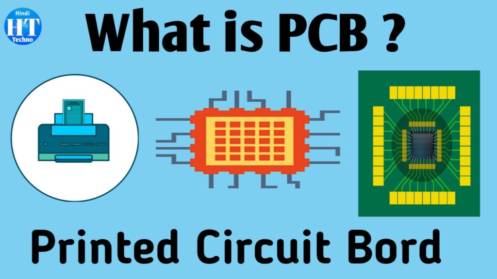
What is PCB?
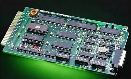
A printed circuit board (PCB) is an electronic circuit used in devices to provide mechanical support and routing to its electronic components.
It is a non-conductive material, such as fiberglass or plastic made by combining different sheets, that easily holds the copper circuitry.
PCB is also known as Printed Wiring Board (PWB) or Etched Wiring Board (EWB).
Printed Circuit Board (PCB Kya Hai? – pcb full form)
PCB is a copper laminated and non-conductive printed circuit board in which all electrical and electronic components are connected together in a common board, with the base of the board having physical support for all components.
When the PCB was not developed, all the components were connected by a single wire which increased the complexity and reduced the reliability of the circuit, thus we could not make very large circuits like the motherboard.
In PCB, all components are connected without wires, all components are internally connected, hence reducing the complexity of overall circuit design.
The PCB is used to provide power and connectivity between components, by which it functions in the way it was designed.
PCB can be customized to any specifications as per user requirements.
It can be found in many electronics devices such as; Such as TV, mobile, digital camera, computer parts; Graphic card, motherboard, etc.
Don’t Miss : cdpo full form
Simultaneously it is used in many fields : Such as pcb full form
- medical equipment
- industrial machinery
- automotive industry
- lighting
PCB ka full form kya hai?
PCB ka full form hindi me “प्रिंटेड सर्किट बोर्ड” OR pcb full form “Printed Circuit Board”.
Types of PCB & pcb full form
There are many types of PCBs available for circuits.
Out of these types of PCBs, we need to choose the suitable type of PCB as per our application.
1) Single Layer PCB:
Single layer PCB is also stands as single sided PCB. This type of PCB is the simplest and most commonly used PCB as these PCBs are easy to design and manufacture.
One side of this PCB is coated with a layer of any conducting material. Generally, copper is used as a conducting material for PCBs, as copper has very good conducting characteristics.
In this type of PCB, only one side of the PCB is used to connect various types of electrical or electronics components such as resistors, capacitors, inductors, etc.
These components are soldered. These PCBs are used in low cost and bulk manufacturing applications such as calculators, radios, printers and solid-state drives.
2) Double Layer PCB:
Double Layer PCB is also known as Double Sided PCB. As the name suggests, in this type of PCB, a thin layer of conducting material,
such as copper, is applied to both the top and bottom of the board. In PCBs, the through consists of a through, on different layers of the board, with two pads in the respective positions on the different layers.
These are connected electrically through a hole in the board, which is shown in the figure.
More flexible, relatively low cost, and the most important advantage of this type of PCB board is its small size which makes the circuit compact.
This type of PCB is mostly used in industrial controls, converters, UPS systems, HVAC applications, phones, amplifiers and power monitoring systems.
3) Multi-Layer PCB:
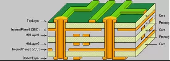
Multi-layer PCB has more than two layers. This means that this type of PCB has at least three conducting layers of copper.
To secure the board, the glue is sandwiched between layers of insulation ensuring that the excess heat will not damage any components in the circuit.
This type of PCB designing is very complex and is used in very complex and large electrical work in very small space and compact circuits.
This type of PCB is used in large applications such as GPS technology, satellite systems, medical equipment, file servers and data storage.
4) Flexible PCB:
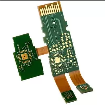
Flexible PCB is also known as flex circuit. Flexible plastic materials such as polyimide, PEEK (polyether ether ketone) or transparent conductive polyester film are used in this type of PCB.
The circuit board is generally folded or twisted.
It is a very complex type of PCB and consists of different layers like single sided flex circuit, double sided flex circuit and multi sided flex circuit.
Flex circuits are used in organic light emitting diodes, LCD fabrication, flex solar cells, automotive industries, cellular telephones, cameras and complex electronics devices such as laptops.
5) Rigid PCB:
Rigid PCBs are made of solid materials that prevent the PCB from being twisted. An demo of a Rigid PCB is a simple computer best motherboard.
Similar as Flex PCB, Rigid PCB has different layer configurations such as single layer, double layer and multi-layer Rigid PCB. The default size of this main PCB does not update after any installation.
This PCB cannot be bent according to the shape of the base, so this PCB is known as RIGID PCB.
This type of PCB has a very long life, so it is used in many parts of the computer such as RAM, GPU and CPU. Simplest in design and most commonly used and most manufacturing PCB is single sided rigid PCB.
Multi-layer rigid PCBs with 9-10 layers can be more compact.
6) Flex-rigid PCB:
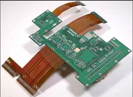
The most important board is composed of a combination of flexible circuit and rigid circuit.
Flex-rigid boards consist of several layers of flexible PCBs connected to multiple rigid PCB layers. Flex-rigid board as shown in the picture.
It is used in cell phones, digital cameras and automobiles etc.
Types of PCBs According to Mounting System
Also Learn to : pcb full form
1) Through-hole PCB:
In this type of PCB, we have to make holes on the PCB using a drill. In these holes, the component leads are mounted and soldered to pads located on opposite sides of the PCB.
This technique is most useful as it provides more mechanical support to the electrical component and is a very reliable technique for component mounting but drilling into the PCB makes it more expensive.
In single layer PCB, this mounting technology is easy to implement, but in case of double layer and multi-layer PCB making holes is more difficult.
2) Surface mounted PCB:
In this type of PCB, the components are smaller in size because these components have very little lead or require no leads to be mounted on the board.
Here, in this technique, the SMD components are placed directly on the surface of the board and there is no need to make holes on the board.
Different Parts of PCB
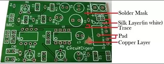
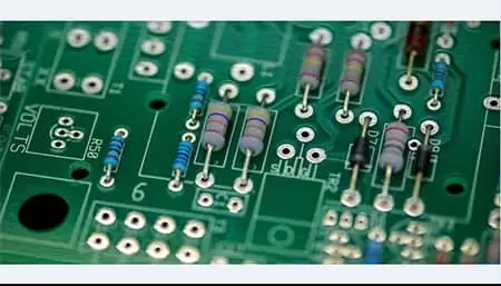
1) Pad:
The pad is nothing but a piece of copper on which the component lids are mounted and on which the soldering is done.
The pad provides mechanical support to the component.
2) Trace:
In PCB, the components are not connected with the help of wires.
All components are connected by a conducting material such as copper.
This copper part of PCB which is used to connect all the components is known as trace.
3) Layers:
According to the application, cost and available space, the user can choose the layer of PCB.
Simplest to manufacture, easy to design and most useful in regular life is Single Layer PCB.
But for very large and complex circuits, double layer PCB or multi layer PCB is most preferred as compared to single layer PCB.
Now a days, in multi-layer PCB, 10-12 layers can be connected and most importantly communication between components in different layers.
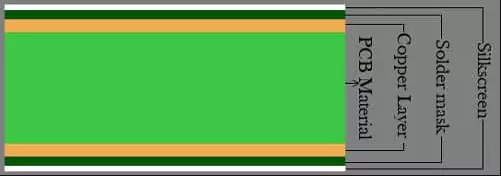
4) Silk layer:
Silk layer is used for printed line, text or any art on the surface of PCB.
Typically, epoxy inks are used for screen printing.
Silk layer can be used on top and/or bottom layer of PCB as per user requirement which is known as silk screen TOP and silk screen BOTTOM.
5) Top and bottom layer:
In the top layer of the PCB, all the components are mounted. Usually, this layer is green.
In the bottom layer of the PCB, all the components are soldered through and the lid of the component is known as the bottom layer of the PCB.
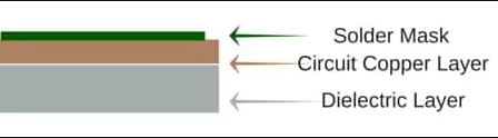
Sometimes, PCBs in the top and/or bottom layers are coated with a green layer, known as a solder mask.
6) Solder Mask:
On top of the copper layer there is an additional layer called a solder mask. This layer is usually green in color but can be any color.
This insulating layer is used on the PCB to prevent accidental contact of the pads with other conductive materials.
PCB Materials:
The main element is the dielectric substrate which is rigid or flexible. This dielectric substrate is used with a conductive material such as copper on it. As dielectric substrates, glass epoxy laminates or composite materials are used.
1) FR4:
FR stands for FIRE RETARDENT. For all types of PCB manufacturing, the most common glass laminated material is FR4. Based on a woven glass-epoxy compound, FR4 is a composite material that is most useful because it provides very good mechanical strength.
2) FR-1 and FR-2:
This material is made from paper and phenol compound and this material is only used for single layer PCB. FR1 and FR2 both have the same characteristic, the only difference is in the glass transition temperature.
FR1 has a higher glass transition temperature than FR2. These materials are divided into standard, halogen free and non-hydrophobic.
3) CEM-1:
This material is made from paper and two layer woven glass epoxy and phenol compound and this material is used only for single sided PCB. CEM-1 can be used instead of FR4, but CEM1 costs more than FR4.
4) CEM-3:
This material is a white colored, glass epoxy compound that is mostly used in double layer PCBs. The CEM-3 has less mechanical power than the FR4, but is cheaper than the FR4. So, it is a good alternative to FR4.
5) Polyimide:
This material is used in flexible PCBs. This material is made from Capton, Rogers, DuPont.
This material has good electrical properties, ductility, wide temperature range and high chemical resistance. The working temperature of this material is -200 degree centigrade to degree centigrade.
6) Prepreg:
Prepreg means pre-important. It is fiberglass with resin. These resins are pre-dried, so that when it is heated, it flows, sticks and completely sinks.
Prepreg has an adhesive layer that gives strength similar to FR4. There are several versions of this material according to the resin material, SR – standard resin, MR – medium resin and HR – high resin.
It is selected according to the required thickness, layer structure and impedance. This material is also available in high glass transition temperature and halogen free.
PCB designing software:
Below are some of the most popular PCB design software. You can learn more about these PCB design software here.
1) Eagle:
EAGLE is the most popular and easiest way to design PCBs. EAGLE stands for Easily Applicable Graphical Layout Editor which is first developed by Cadsoft Computer and currently Autodesk is the developer of this software.
2) Multisim:
Multisim is also very powerful and easy to learn software. Originally developed by Electronics Workbench and now a division of National Instruments (NI).
This includes microcontroller simulation (MultiMCU) and import export features integrated into the PCB layout software. This software is widely used for circuit education in academia and industry as well.
3) EasyEDA:
EasyEDA is a software used to design and simulate circuits. This software is an integrated tool for schematic capture, SPICE circuit simulation based on Ngspice and PCB layout. The most important advantage of this software is that, it is web base software and is used in the browser window.
4) Altium Designer:
This software is developed by Australian software company Altium Limited. The main feature of this software is schematic capture, 3D PCB design, FPGA development and release/data management.
It is the first software to offer 3D visualization and clearance checking of PCBs directly from the PCB editor.
5) KiCad:
This software is developed by Jean-Pierre Charn. The software has tools that can create BoM (Bill of Materials), artwork and 3D views of PCBs as well as all the components used in circuits.
There are many components available in the library of this software and there is such a facility that users can add their own custom components. This software supports many languages.
Thanks a lot for my best post “pcb full form” – Printed Circuit Board. Please share your friends.